Inside every semiconductor chip, transistors are wired together by interconnects thinner than one ten-thousandth the width of a human hair. Copper (Cu) has been the workhorse material for these wires for decades, but it is now running into a physical wall as chips keep shrinking. At the VLSI Symposium, an international conference held in Kyoto in June 2025, Tokyo Electron and imec, the Belgium-based research institute, jointly presented new research into what could replace copper in future chips. Their presentation offers a window into where interconnect technology is headed next.
Why copper wiring is nearing its limit
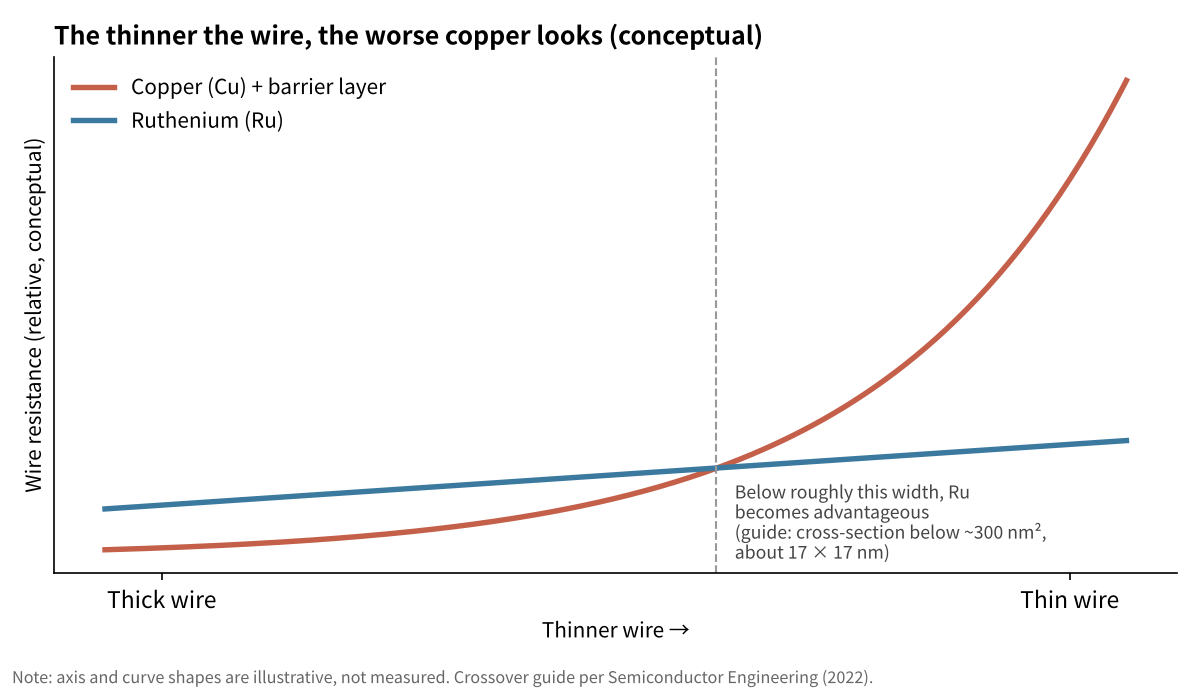
Copper has long been the default choice for on-chip wiring because it conducts electricity well and is relatively easy to process. But once wire widths shrink to around 40 nanometers (nm; one nanometer is one-billionth of a meter) or below, copper’s resistance actually starts to rise rather than fall. As wires get thinner, electrons collide more often with the wire’s surface and with the boundaries between metal grains, making it harder for current to flow smoothly. Higher resistance means slower signals and higher power consumption. Since further miniaturization is inevitable, finding a replacement for copper has become a shared challenge across the industry.
The presentation: ruthenium and semi-damascene wiring
The joint presentation by Tokyo Electron and imec at VLSI 2025 was titled “Selective Deposition and Ruthenium Superfill for A10-and-Beyond Interconnects.” Ruthenium (Ru) is drawing attention as a metal whose resistance rises more gradually than copper’s as wires get thinner.
The key idea is a fabrication approach called “semi-damascene.” Conventional copper wiring has relied mainly on the “damascene” process: a trench is etched into the insulating layer first, then filled with metal, and the surface is polished flat. Semi-damascene works differently. A metal film is first deposited across the entire wiring layer, and the unwanted portions are then removed by etching to directly carve out the wiring pattern, skipping the trench-and-fill step altogether. This makes it easier to build the finer, more three-dimensional wiring structures that future chips will need. The new presentation outlined a technical path for depositing ruthenium evenly, even into the narrowest gaps, when this process is used, a property known as “superfill.”
Why this matters
In AI chips packed densely with computing circuits, power loss and signal delay in the interconnects can limit the performance of the entire chip. The fact that Tokyo Electron, an equipment maker, is co-developing the interconnect process itself with imec, a materials research hub, signals something important: the practical realization of next-generation interconnects is no longer just about sourcing the right material, it has become a contest over deposition and processing equipment technology.
AI computation depends on huge numbers of transistors exchanging large amounts of data. Even if transistors get faster, high wire resistance delays signals and increases heat and power use. Interconnects are like the roads of a chip, and their quality helps determine overall performance. That is why the search for a copper replacement is as important to semiconductor progress as transistor scaling itself.
Why ruthenium looks promising
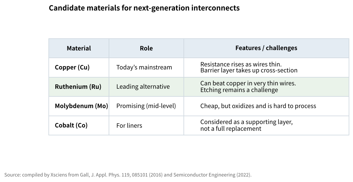
As an interconnect material, copper becomes less attractive the thinner it gets. In a talk at IEDM 2020 (summarized in a series by EE Times Japan), imec compared the resistance of vias, the vertical connections between wiring layers. Taking a 14 nm copper via with a 2 nm barrier layer as the reference value of 1, a 10 nm copper via comes to 2.16, more than double, while ruthenium was calculated at 0.59 at 14 nm without a barrier layer. These are calculated comparisons that assume particular dimensions and structures, not direct measurements of actual products. Ruthenium is valued because its resistance is low, it does not need the barrier layer (a thin film that stops copper from diffusing into surrounding insulation) that copper requires, and it can be shaped by etching.
imec’s 16 nm-pitch ruthenium lines
On June 3, 2025, imec reported, in a presentation at the IITC 2025 conference, ruthenium lines at 16 nm pitch made with a semi-damascene process. The average resistance was 656 ohms per micrometer, and 40% of the 16 nm-pitch structures met the target resistance predicted from thin-film resistivity (corresponding to 8 nm-wide local wiring). At 18 to 22 nm pitch, full-wafer yield of more than 90% was reported. The work targets the first local wiring layer (M0) of logic chips from the A7 generation onward. This was a different conference from the VLSI Symposium presentation by Tokyo Electron and imec described above.
Hurdles before real-world use
Even in imec’s report, only 40% of structures at 16 nm pitch met the target resistance, and yields above 90% were obtained in the 18 to 22 nm pitch range. Remaining issues include optimizing the patterning of ruthenium and suppressing changes in its shape caused by heat. Replacing copper with ruthenium is still at the research stage.
Xsciens Editorial Note
“Copper to ruthenium” is not a done deal; it is a research question about where copper’s limit sits and which materials could take over beyond it.
- Results versus mass production. What the conference presentations show are research-stage results. Independent work agrees that the direction is plausible: a materials study from Rensselaer Polytechnic Institute (Gall, 2016) found that some metals such as rhodium, iridium and nickel can outperform copper in very narrow wires, while molybdenum, cobalt and ruthenium roughly match it, so ruthenium is one candidate among several.
- The crossover is a guide, not a line. A commonly cited guide is that ruthenium becomes less resistive than copper below a cross-section of roughly 300 nm² (about 17 × 17 nm), but the exact point depends on barrier thickness, grain structure and process. The figure in this article is a conceptual schematic, not measured data.
- What to watch next. Etching without damaging the metal (oxidation is a known challenge), uniformity across a whole wafer, cost, and whether cheaper options such as molybdenum take the middle layers while ruthenium takes the thinnest ones.
- Our imagination (speculation) — We wonder whether this kind of wiring change might eventually let phones and data centers do the same computing with less wasted heat, which could mean longer battery life or lower cooling needs. But a new material also brings new factory processes and costs, so how much of this reaches everyday products is still unknown. This is our speculation, not a forecast.
References for this note: Gall, “Electron mean free path in elemental metals”, Journal of Applied Physics 119, 085101 (2016) (Rensselaer Polytechnic Institute), Semiconductor Engineering, “How Far Will Copper Interconnects Scale?” (Dec 15, 2022)
Key terms
- Pitch: the distance between the centers of neighboring wires
- Via: a vertical connection between upper and lower wiring layers
- Barrier layer: a thin film that keeps copper from diffusing into the surrounding insulating film
- Superfill: deposition that fills even narrow trenches and gaps with metal evenly
- A10, A7: names for next-generation chip nodes (the letter A stands for the angstrom, one tenth of a nanometer); they do not necessarily indicate an actual physical dimension
Whether copper will actually be replaced by ruthenium in chip wiring remains a research question, not a settled fact. But tracking what gets presented at international conferences like this one reveals where the next bottlenecks in semiconductor scaling lie, and where equipment makers are looking for solutions. The unglamorous work of wiring a chip is turning out to be one of the front lines that will determine how far AI-era chip performance can go.
Sources: Tokyo Electron Newsroom, “2025 IEEE Symposium on VLSI Technology and Circuits”, imec, “Semi-damascene metallization: an inflection point in back-end-of-line processing”, imec press release (June 3, 2025), EE Times Japan
Leave a Reply