Category: Uncategorized

  • [Economy] Engineers Who Skip the Patent System Are Leaving Pay and Credit on the Table: A Practical Guide

    Do you think of patents as “the IP department’s job” or “something for patent attorneys”? In reality, an engineer who doesn’t understand the patent system can end up missing out on compensation and career credit they’re legally entitled to — often without ever realizing it. The good news is that a few small habits are enough to turn your own technical work into fair compensation and a career asset. This guide covers the patent basics, then four things you can start practicing tomorrow, plus a daily checklist.

    0. The Patent Basics to Know First

    To be patentable, an invention generally needs three things: novelty (it doesn’t already exist in the world), an inventive step (a specialist in the field wouldn’t easily come up with it), and industrial applicability.

    The path from filing to a granted right runs: file the application → publication (automatically, 18 months after filing) → request for examination (you must request this yourself within 3 years of filing, or it’s never examined) → substantive examination → decision to grant → registration. If you never request examination, the invention’s contents simply become public — it never becomes an enforceable right.

    The single most important part of a patent is its “claims” — the scope of what’s legally protected. This is where the breadth and strength of the right is decided. No matter how detailed the written description is, any technology not captured in the claims isn’t protected.
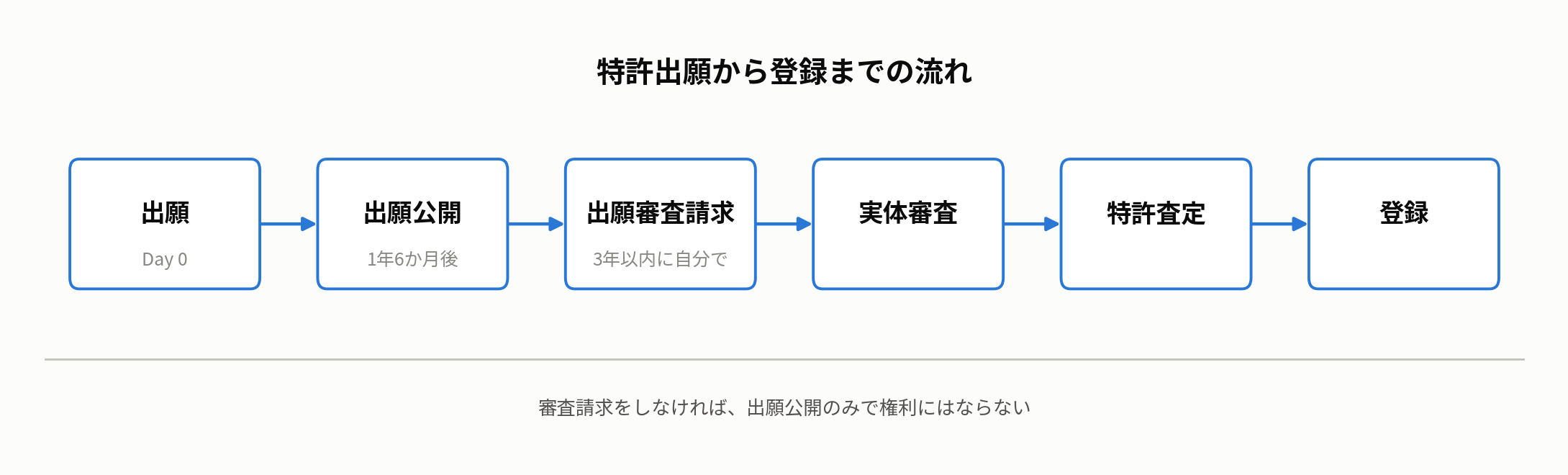
    Diagram of the patent lifecycle: filing, publication, request for examination, substantive examination, decision to grant, registration
    The standard path from filing to registration. Note that examination never starts unless you request it yourself.

    1. Make Prior-Art Search Step One of Any New Project

    Running a patent search before starting a new project heads off two problems at once:

    • Reinventing the wheel: you avoid spending time building something that already exists, simply because you didn’t know about it.
    • Freedom-to-Operate (FTO) risk: discovering that a competitor already holds a patent on your approach, after the fact, can force a costly redesign or expose you to infringement risk.

    Japanese patent data can be searched for free, with no registration required, through J-PlatPat (the Japan Platform for Patent Information). As a beginner, three kinds of search will get you most of the way:

    • Keyword search — technical terms have multiple names, so connect synonyms with OR (e.g., “artificial intelligence OR AI OR machine learning”).
    • Applicant search — search by the name of a competitor or a related research institution to see which technologies they’re investing in.
    • FI/F-term (patent classification) search — use the classification codes the Japan Patent Office assigns to narrow down technical fields that keywords alone can’t capture.

    2. Read Patent Gazettes as a “Catalog of the Latest Technology”

    A patent gazette — especially the “published unexamined application” that comes out 18 months after filing — is a primary source packed with cutting-edge technical information that hasn’t made it into papers yet. You don’t need to read it cover to cover; reading in this order is efficient:

    • Abstract — grasp the gist of the invention in a few hundred characters.
    • Claims — check the scope the patent actually protects. Comparing this against your own design is the basis of an FTO check.
    • Description and drawings — for patents you’re genuinely interested in, dig into implementation details and examples.

    Even just tracking how filing volume in a given field is trending, or which companies are filing heavily on which technologies, tells you a lot about where the industry’s effort is going.

    3. Turn Ideas Into an “Invention Proposal” as Soon as They Come to You

    Even a great idea, if it’s only ever spoken aloud, leaves no record and never becomes a patent. Many companies follow an internal process like this:

    • The moment an idea occurs to you, jot down the date, the problem, the solution, and the effect — a notebook or an internal system is fine.
    • Propose it to your manager or IP staff using the company’s “invention proposal” format.
    • An internal invention review board judges whether it’s worth filing.
    • If it moves forward, you work with a patent attorney to build out the claims and description — and this is where it matters that the engineer conveys the technical content accurately.

    This is where Japan’s “employee invention system” (Article 35 of the Patent Act) comes in. Under the 2015 revision, if a company has specified in advance — through a contract or work rules — that it will acquire the right to obtain a patent, that right belongs to the company from the moment the invention is made. In exchange, the inventing employee is entitled to receive “reasonable benefit.” This isn’t limited to money — it can include other economic benefits under the company’s own programs, such as opportunities to study abroad or a promotion or award.

    Even when the right to a patent defaults to the company, Article 35 of Japan’s Patent Act guarantees the inventing employee “reasonable benefit” in return. Proposing an invention isn’t unpaid labor — it’s something the law entitles you to be compensated for.

    4. Turn Patents Into a Career Asset

    • Being named as an inventor is an objective credential that carries weight outside your company too. Patent gazettes list inventors by name, giving you concrete material to point to — “here’s what I created” — when changing jobs or during internal reviews.
    • Many companies run internal invention-recognition programs, rewarding inventions that contribute to commercialization with awards or bonuses.
    • The experience of writing a patent is also training in putting your own technology into words a third party can understand — a skill that raises the quality of your technical writing generally.

    A Practical Checklist

    • Before starting a new project, I’ve run at least one keyword search on J-PlatPat.
    • When an idea occurs to me, I jot down the date, the problem, and the solution on the spot.
    • I check the claims of competitors’ patents in technology close to our own products, and I’m aware of the infringement risk.
    • I know my company’s invention-proposal format and where to submit it.
    • I’ve at least once read through my company’s employee-invention rules (what counts as “reasonable benefit”).

    The essence of using patents well comes down to three unglamorous habits: record your ideas, search first, and read the claims. None of these require special skill — you can start today with nothing more than a notebook and a browser. Building patents into your own development process, rather than leaving them entirely to the IP department, looks like the long way around but is actually the shortest path.

    Japan Patent Office, “Overview of the Employee Invention System”
    Japan Patent Office, J-PlatPat (Patent Information Platform)
  • [Science] RIKEN Focuses an Attosecond Laser 100 Times Tighter — From Watching Electrons Move to Putting That Motion to Work

    A team at Japan’s RIKEN institute has focused an “attosecond laser” — a flash of light lasting a mere quintillionth of a second — onto a spot smaller than a micrometer, at more than 100 times the intensity previous tabletop sources achieved. The team frames the advance as a shift from simply watching how electrons move inside matter to actively putting that motion to work. Down the road, the underlying technology could feed into nanoscale material processing and research on next-generation electronic materials and devices.

    原論文情報 / Original Paper
    Title: Submicrometer Focusing of Isolated Attosecond XUV Pulses Approaching 1016 W/cm2
    Authors: Imasaka, K. et al.
    Journal: Ultrafast Science (2026)
    DOI: 10.34133/ultrafastscience.0198

    What “attosecond science” means

    An attosecond is a quintillionth of a second (10-18 seconds) — a timescale almost impossible to picture. Electrons inside atoms move on exactly this scale, and the technique for capturing that instant won the 2023 Nobel Prize in Physics. What RIKEN produced is an “isolated attosecond pulse,” generated by driving a laser through a process called high-harmonic generation. This new result is a major upgrade to the focusing technology needed to turn that pulse from a tool for observation into one for processing and control.

    A 100-fold jump, a world record for tabletop sources

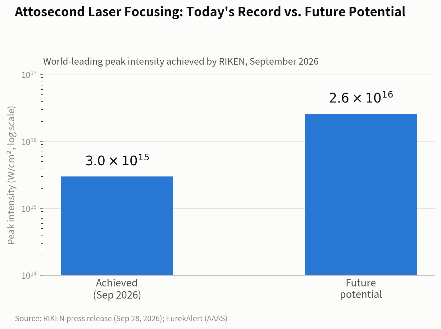
    A team led by Special Postdoctoral Researcher Kotaro Imasaka at RIKEN’s Center for Advanced Photonics built a new elliptical multilayer mirror finished to sub-nanometer surface quality (roughly 0.892 nm RMS roughness), paired with a real-time system that stabilizes the focal point. The result: a focal spot of just 460±130 by 360±120 nanometers — under a micrometer across — reaching a peak intensity of 3.0×10¹⁵ W/cm² (3 quadrillion watts per square centimeter) at the pulse’s peak. That is the highest peak intensity ever reported for an isolated attosecond pulse from a tabletop light source, more than 100 times beyond previous tabletop sources of the same kind.

    The team describes the achievement as opening the door to “a new ultrafast, high-intensity optical science” that moves beyond observing electron motion toward changing and harnessing it.

    EurekAlert, the news service run by the American Association for the Advancement of Science, corroborated the finding, reporting a peak pulse power of 1.1 gigawatts. It added that, with further refinement, the method could in principle reach 2.6×10¹⁶ W/cm² — about 8.7 times today’s figure — though that remains a future projection, not something already achieved. The underlying paper appeared online in the journal Ultrafast Science on September 23, 2026.

    Why it matters

    When light gets intense enough, a material’s response to it stops being simply proportional — unusual effects start to appear. That’s the realm of “nonlinear optics.” With higher intensity and tighter focusing, researchers can now push these nonlinear effects onto the attosecond timescale — “nonlinear attosecond optics” — not just in gases but in solids and liquids too. The team points to nanoscale surface processing and studies of ultrafast electron dynamics inside condensed matter as near-term applications, with possible spillover into future electronic materials and devices further out. For now, though, this remains basic research: turning it into real products or industrial applications will take further work.

    Bar chart showing attosecond laser peak intensity achieved versus future potential
    Source: created from data in RIKEN’s press release and EurekAlert

    Xsciens editorial note: reading the 100-fold claim

    Two qualifiers matter. First, the record is for tabletop sources: laser setups that fit in a laboratory rather than large facilities, so the comparison is with other tabletop systems and not with every attosecond light source in the world. Second, the headline intensity of 3.0×10¹⁵ W/cm² is what was achieved, while the 2.6×10¹⁶ W/cm² reported by EurekAlert is only what refinement could allow in principle, about 8.7 times higher.

    The advance is also in the focusing, not in making a stronger pulse. The team made the pulse hit a spot under a micrometer wide by building a very smooth mirror and keeping the focus stable in real time. That is why the work matters for experiments on solids and liquids, where tightly concentrated light is needed to trigger nonlinear effects. What to watch next is whether the nonlinear attosecond experiments the team describes are actually carried out in condensed matter, since for now this is basic research.

    Key terms

    • Attosecond: one quintillionth of a second, the timescale of electron motion in atoms
    • High-harmonic generation: a process in which an intense laser produces light at much higher frequencies, used to make attosecond pulses
    • Isolated attosecond pulse: a single, extremely short flash of light rather than a train of pulses
    • Nonlinear optics: the realm where a material’s response to light stops being proportional to its intensity
    • Tabletop source: a light source small enough to be built in an ordinary laboratory

    Sources: RIKEN press release, EurekAlert! (AAAS), Ultrafast Science journal article

  • [Economy] A ¥20,000 Invention Bonus, a ¥60.4 Billion Court Valuation: How One Patent Built a Trillion-Yen Business

    What if a single patent could translate into a legal claim worth tens of billions of yen for the individual engineer who invented it? Shuji Nakamura, inventor of the blue LED, originally received an in-house bonus of just ¥20,000 for his work — yet a later court case calculated his personal contribution to the invention at roughly ¥60.4 billion. Patents tend to conjure an abstract image, something like a technologist’s badge of honor. But for both companies and the inventors who work for them, a patent is a genuine money-making mechanism. This piece lays out how patents translate into corporate profit, then looks at one real example of a single patent generating extraordinary value: Nichia Corporation’s blue LED patent.

    What a Patent Actually Is

    A patent is a right the government grants to whoever makes a new invention: the exclusive right to use that invention for a set period. In Japan, for 20 years in principle from the filing date, no one but the patent holder may manufacture or sell that invention without permission. In other words, a patent isn’t the technology itself — it’s an asset representing the right to prevent others from using that technology, or to charge them for the privilege, and that right can be bought, sold, and enforced.

    Four Ways Patents Drive Corporate Profit

    High margins through exclusivity (competitors can’t make the same product, so there’s no price competition and margins stay high); license revenue (a company doesn’t have to manufacture anything itself — it can license the technology to others for royalties); litigation and negotiating leverage (a company can seek damages from unauthorized use, or negotiate settlements from a position of strength); and value as an intangible asset (patents held by a company represent enterprise value that doesn’t show up on the balance sheet, but still factors into stock price, fundraising, and M&A valuations). Of these four, exclusivity-driven high margin is by far the most powerful.

    Case Study: How the Blue LED Patent Built a Trillion-Yen Business

    In 1993, Shuji Nakamura, then an engineer at Nichia Corporation, developed the world’s first practical high-brightness blue LED. Until then, LEDs came only in red and green; adding blue completed the three primary colors of light, making full-color displays possible and enabling white LED lighting (created by combining blue with yellow). White LEDs spread around the world as an energy-efficient alternative to incandescent and fluorescent lighting, and Nichia used its blue LED patents to seize an overwhelming share of the global market.

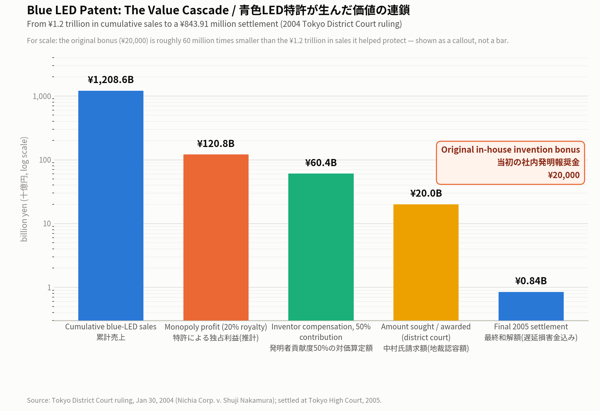
    A 2004 Tokyo District Court ruling put a number on that patent’s worth. Nakamura sued Nichia seeking compensation for his invention under Japan’s employee-invention system, and the court calculated the patent’s value as follows: Nichia’s cumulative blue-LED-related sales came to roughly ¥1.2086 trillion; applying a 20% royalty rate to the portion the patent protected yielded an estimated monopoly profit of roughly ¥120.8 billion; and crediting Nakamura with a 50% contribution to the invention put his compensation at roughly ¥60.4 billion. Of that ¥60.4 billion, the court ordered Nichia to pay the ¥20 billion Nakamura had originally sought. The case was ultimately settled at the Tokyo High Court in 2005, with Nichia paying about ¥843.91 million including delay damages — a steep discount from the district court figure, but still, set against Nakamura’s original in-house invention bonus of just ¥20,000, a striking illustration of how much economic value a single invention and a single patent can carry. In 2014, Nakamura was awarded the Nobel Prize in Physics for the invention.

    Bar chart on a log scale showing the blue LED patent's value cascade: cumulative sales of about ¥1,208.6 billion, an estimated monopoly profit of about ¥120.8 billion, court-calculated inventor compensation of about ¥60.4 billion, the ¥20 billion Nakamura sought, and the final settlement of about ¥843.91 million, with the original ¥20,000 in-house bonus called out separately.
    Figures from the 2004 Tokyo District Court ruling (log scale, billion yen). Note the gap versus the original ¥20,000 in-house bonus. Source: Tokyo District Court ruling, Jan 30, 2004.
    The original in-house invention bonus was ¥20,000. The court’s own calculation of Nakamura’s contribution came to roughly ¥60.4 billion — a gap of about three million times.

    How Japan’s Employee-Invention Rules Changed Afterward

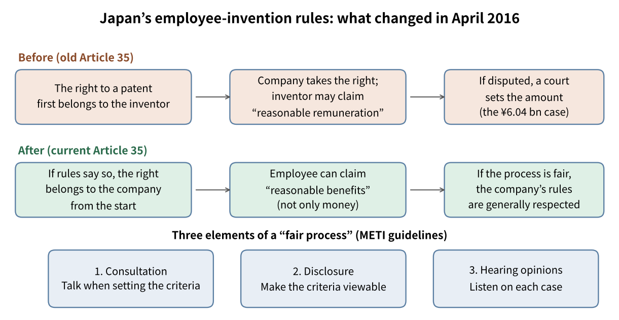
    Employee inventions are governed by Article 35 of Japan’s Patent Act. Under the 2015 amendment (in force from April 1, 2016), if a contract or work rules state in advance that the company acquires the rights, the right to obtain a patent belongs to the company from the moment the invention is made (Article 35, paragraph 3). Before the amendment, the right first belonged to the inventor and the company took it over. The change was meant to remove the complications that arise in joint research and the risk of an inventor assigning the same rights to a third party.

    Employees still keep the right to receive a “reasonable benefit” (paragraph 4). Such a benefit is not limited to money: stock options, promotions, paid leave beyond what the law or work rules require, and study-abroad opportunities can count, but a mere certificate of commendation does not. When a company sets standards for the benefit in a contract or work rules, giving benefits under those standards must not be found unreasonable (paragraph 5). In judging that, the process is taken into account in three steps: consultation when the standards were set, disclosure of the standards, and hearing the employee’s opinion when the benefit for an individual invention is decided. If these steps were handled properly, the company’s standards are respected. The Minister of Economy, Trade and Industry issues guidelines on proper procedure (paragraph 6).

    Five Points to Check in Your Own Company’s Rules

    • Does a contract or the work rules state that the company acquires the rights from the start?
    • Was there an opportunity to consult with employees when the standards for the benefit were set?
    • Are the standards disclosed so that employees can read them, with specific content and conditions?
    • Can employees state opinions or objections when the benefit for an individual invention is decided?
    • If the benefit is not money, is its content specified?

    Inventions made before April 1, 2016 are in principle covered by the old law, and those made on or after that date by the amended law. For a specific case, consult your company’s intellectual property department or a patent attorney or lawyer. This article is general information, not legal advice.

    The Rest of Article 35: Non-Exclusive License and How Benefits Are Valued

    Paragraph 1 provides that even when an employee obtains a patent on an employee invention, the company holds a non-exclusive license to use it free of charge. The idea is that the company provided the research environment and equipment.

    Paragraph 2 makes void any contract or work rule that gives the company advance rights to inventions that are not employee inventions. A company cannot, by rule, automatically own an individual’s invention unrelated to the job.

    Paragraph 7 covers cases in which no standard exists, or in which giving the benefit as the standard provides is found unreasonable under paragraph 5. In that case the content of the reasonable benefit must be decided by considering the profit the company earns from the invention, the burden the company bears in connection with it, the contribution of the company and the inventor, and the treatment of the employee. This is the logic of comparing the value of the invention with each side’s contribution, and it is the idea that comes into play when amounts are disputed.

    Before and after the 2016 amendment of Japan’s employee-invention rules, and the three elements of a fair process
    Before and after the amendment, and the three elements of a “fair process” (diagram by Xsciens based on the JPO overview).

    The Bottom Line

    A patent is a certificate of technical achievement, but it’s also a business asset that feeds directly into company profit through exclusivity, licensing, litigation leverage, and enterprise value. As the blue LED case shows, being first to lock up a genuinely pivotal technology with a patent can be enough, on its own, to build a trillion-yen business — and, as Nakamura’s case shows, can turn a single engineer’s idea into a legal claim worth tens of billions of yen. That’s exactly why companies pour as much energy into patent strategy as they do into R&D itself.

    Xsciens Editorial Note

    The striking “¥20,000 to ¥60.4 billion” figure is real, but the more important story is what happened afterward: the rules themselves changed.

    • A court’s calculation is not money received. As the article notes, the case was settled on appeal for roughly ¥840 million. Remembering only the headline number gives the wrong picture of how the system works.
    • The focus moved from the amount to the process. Under the amendment effective April 2016, if the process (consultation, disclosure and hearing of opinions) is fair, a company’s own rules are generally respected. In principle, that leaves fewer situations in which a court decides the amount afterward.
    • What we still cannot tell. A proper process does not by itself tell us whether the resulting criteria feel fair to employees. That depends on how each company operates.
    • Our imagination (speculation) — We wonder whether, for people who will invent things in the future, reading the company’s invention rules once when joining may matter more than a famous court figure. Knowing the criteria before results appear is likely easier than arguing after them. This is only our speculation, and individual contracts and rules differ widely.

    References for this note: Japan Patent Office, “Overview of the Employee Invention System” (in Japanese; 2015 amendment effective April 2016, “reasonable benefits”, consultation / disclosure / hearing of opinions)

    Tokyo District Court, judgment of January 30, 2004 (the blue LED compensation lawsuit, Nichia Corporation v. Shuji Nakamura)
    ITmedia NEWS, “Blue LED Lawsuit: Nichia Settles for ¥843.91 Million”
    Nichia Corporation, “Settlement in Tokyo High Court Case No. 962 (ne) and No. 2177 of Heisei 16”

  • [Economy] Japan Doesn’t Make the Chips — It Makes the Machines That Make Them, and Leads the World in Patents Too

    The most advanced chips in your phone, your car, and the AI models running in the cloud are usually associated with Taiwan or South Korea — but only a handful of countries can supply the machines that make those chips in the first place. Japan quietly controls this chokepoint in the global semiconductor supply chain, with companies like Tokyo Electron, SCREEN Holdings, and DISCO ranking among the world’s top makers of semiconductor manufacturing equipment. That strength shows up just as clearly in the patent world. Drawing on data from the Japan Patent Office and specialist patent-analytics firms, here’s a look at Japanese equipment makers’ patent trends, what they reveal, and one especially notable patent.

    World-Leading in Both Patent Quantity and Quality

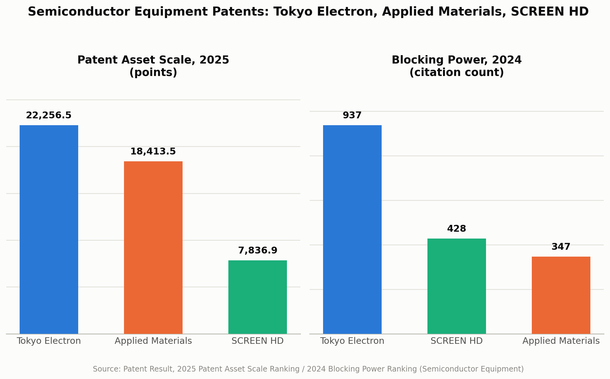
    In the “2025 Patent Asset Scale Ranking for the Semiconductor Equipment Industry,” published by the patent analytics firm Patent Result, Tokyo Electron ranked first in the world with 814 registered patents and a score of 22,256.5 points. Applied Materials of the US came in second (586 patents, 18,413.5 points), and SCREEN Holdings placed third (329 patents, 7,836.9 points). This “patent asset scale” isn’t a simple count of filings — it’s calculated by multiplying each patent’s prominence (such as how often it’s cited) by its remaining term, so it measures not just volume but how many genuinely impactful patents a company holds.

    Even more interesting is the 2024 “Blocking Power Ranking.” This tallies how many times a company’s patents were actually cited by examiners as prior art when rejecting other companies’ applications. Here too, Tokyo Electron topped the list with 937 citations, followed by SCREEN Holdings (428), Applied Materials (347), DISCO (277), and ULVAC (154) — Japanese companies took four of the top five spots. The more often a rival’s new invention gets bounced back with, in effect, “we already patented that,” the more that company’s technology has become foundational to the industry.

    Ranking (Year)1st2nd3rd
    Patent Asset Scale (2025)Tokyo ElectronApplied MaterialsSCREEN HD
    Blocking Power (2024)Tokyo ElectronSCREEN HDApplied Materials
    Bar chart comparing Tokyo Electron, Applied Materials, and SCREEN Holdings on 2025 Patent Asset Scale points and 2024 Blocking Power citation counts
    Source: Patent Result, 2025 Patent Asset Scale Ranking and 2024 Blocking Power Ranking (semiconductor equipment industry)

    Three Things the Patent Data Reveals

    1. Citation counts matter more than filing volume as a measure of real strength.
    In a field like semiconductor equipment, where technology builds cumulatively, foundational inventions with broad applicability tend to get cited again and again as grounds for rejecting later filings. Tokyo Electron topping both rankings isn’t just about filing a lot of patents — it’s evidence the company holds foundational technology that rivals simply can’t route around.

    2. Strength is concentrated in front-end processes (deposition, etching, cleaning).
    Looking at the substance of the top-ranked patents, most cluster around “front-end” technologies that work directly on the wafer — deposition, etching, and cleaning. As chips keep shrinking, the value of nanometer-precision processing and cleaning technology keeps rising, so depth of patents in this area translates directly into competitiveness.

    3. These companies have been filing with a global market in mind from the start.
    According to Tokyo Electron’s own disclosures, the company has maintained a global patent filing rate — the share of patents also filed overseas — of roughly 75% for six consecutive years. Securing rights simultaneously not just in Japan but in the major chipmaking countries and regions (the US, China, South Korea, Taiwan) reflects a filing strategy that tracks the company’s global market share.

    One Standout Patent: A Cleaning-Equipment Patent That’s the Industry’s Biggest “Wall”

    A patent’s value isn’t just about how many there are — it’s also about how much it blocks competitors from filing around it. A good example is Tokyo Electron’s patent covering technology that cleans a wafer’s front surface, its beveled edge (the angled cut at the rim), and its back surface all in a single cleaning tool. According to Patent Result’s 2024 survey, this patent was cited more often than any other as grounds for rejection in competitors’ patent examinations — meaning rival makers’ new cleaning-technology filings have repeatedly run into this one idea.

    Cleaning may sound like an unglamorous step, but a semiconductor becomes defective the moment a single invisible speck of dust lands on it. The idea of efficiently cleaning three differently shaped surfaces — front, back, and edge — in one machine is a foundational technology whose value only grows as miniaturization advances. It’s a good example of an unflashy technology that quietly props up the industry from behind the scenes.

    The Bottom Line

    Behind the flashy headlines about semiconductors themselves, the Japanese companies that build the machines that make them maintain a world-class presence in patents, both in quantity and quality. As demand for AI and leading-edge logic chips keeps growing, the patent competition around front-end technologies like deposition, etching, and cleaning looks set to intensify further.

    Patent Result, “2025 Patent Asset Scale Ranking for the Semiconductor Equipment Industry: Top 3 Are Tokyo Electron, AMAT, and SCREEN”
    Patent Result, “2024 Blocking Power Ranking for the Semiconductor Equipment Industry: Top 3 Are Tokyo Electron, SCREEN, and AMAT”
    Tokyo Electron, “Intellectual Property and Intangible Assets”

  • Turning Air Into Ammonia, More Gently — Kyoto University Team Explains Why a Molybdenum Catalyst Works

    Ammonia is the backbone of the world’s food supply as the raw material for fertilizer, but making it burns a staggering amount of energy worldwide. A research team including Kyoto University’s Fukui Institute for Fundamental Chemistry has now worked out the previously unknown mechanism behind a molecular catalyst that converts nitrogen gas (N2) — abundant in the air around us — into ammonia under comparatively mild conditions.

    A Process That Eats 1-2% of the World’s Energy

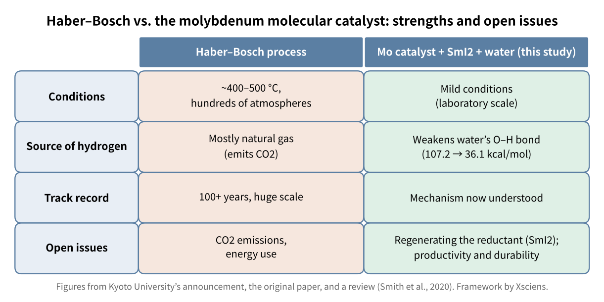
    Today, almost all industrial ammonia comes from the Haber-Bosch process, which forces nitrogen and hydrogen to react at roughly 400–500°C and hundreds of atmospheres of pressure. Because the hydrogen feedstock is mostly made from natural gas, the process comes with heavy CO2 emissions. Global ammonia production is estimated to account for something like 1–2% of the world’s total energy consumption, and chemists have long sought a way to fix nitrogen under gentler conditions.

    Turning Water Into a “Powerful Hydrogen Carrier”

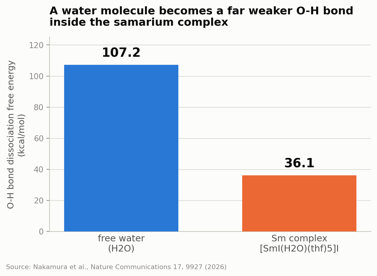
    The team focused on a reaction system that pairs a molybdenum (Mo) molecular catalyst with samarium diiodide (SmI2) and water. Normally, breaking water’s O-H bond to hand off a hydrogen — in chemical terms, a proton and an electron delivered together in a process called proton-coupled electron transfer (PCET) — takes a large amount of energy. But through theoretical calculations, the team found that when water binds to a samarium ion to form the complex [SmI(H2O)(thf)5]I, that O-H bond’s dissociation free energy drops dramatically.

    The O-H bond dissociation free energy of a free water molecule is 107.2 kcal/mol, but inside the samarium complex it falls to 36.1 kcal/mol — down to roughly a third, by calculation.
    Bar chart comparing O-H bond dissociation free energy of free water versus water in the samarium complex
    Figure: O-H bond dissociation free energy (BDFE) of water, free vs. bound in the samarium complex — 107.2 kcal/mol down to 36.1 kcal/mol. Source: Nakamura et al., Nature Communications 17, 9927 (2026)

    Mapping the Reaction Pathway for the First Time

    Combining experiments with theoretical calculations, the team also worked out the step-by-step pathway by which nitrogen on the molybdenum center transforms — from nitride (Mo≡N) to imide (Mo=NH) to amide (Mo-NH2) and finally to an ammonia complex. The step demanding the most energy, by calculation, was imide formation, with an activation free energy of 5.1 kcal/mol. Structural models corresponding to the imide and amide species — related compounds carrying a methyl group on nitrogen — were actually isolated and had their structures determined.

    Why It Matters

    With the reaction mechanism now mapped out, the team has a design roadmap for improving the catalyst further. A related molecular catalyst the same team has previously developed has produced as many as 60,000 equivalents of ammonia per molybdenum atom, and the new mechanistic insight is expected to feed into next-generation nitrogen-fixation technology. The findings were published in Nature Communications on September 24, 2026.

    Comparison table of the Haber–Bosch process and the molybdenum molecular catalyst: conditions, hydrogen source, track record and open issues
    Comparison of the industrial process and this catalyst (compiled by Xsciens from Kyoto University’s announcement, the paper and a review).

    The Team and Where This Work Fits

    The research was carried out by Kazunari Yoshizawa of Kyoto University’s Fukui Institute for Fundamental Chemistry (professor emeritus at Kyushu University), Professor Yoshiaki Nishibayashi of the University of Tokyo’s Graduate School of Engineering, Professor Hiromasa Tanaka of Daido University, and Assistant Professor Taiji Nakamura of Kyoto Institute of Technology, among others. Nishibayashi’s group had earlier reported that a molybdenum molecular catalyst can make ammonia from nitrogen and water at ordinary temperature and pressure (the reaction system also uses samarium diiodide). This time the team tackled the question of why that reaction proceeds.

    Experiments and Calculations Working Together

    The team isolated reaction intermediates, the species formed partway through the reaction, as stable compounds and confirmed their structures, which backed the proposed pathway experimentally. They also used quantum chemical calculations (computer methods that predict how molecules behave from quantum mechanics) to examine steps that are hard to observe directly, confirming the structure of the samarium diiodide and water complex and the important role of proton-coupled electron transfer in forming ammonia. According to Kyoto University, the hardest step in the whole reaction is the one that forms the imide.

    Hurdles Before Practical Use

    The result is an understanding of how the reaction works, and it does not by itself become an industrial production method. Using this understanding as a clue, the group aims to develop high-performance catalysts that make ammonia with less energy. It also says that sustainable ammonia production needs not only better catalysts but also work on reaction conditions to enable renewable energy use and lower production costs.

    According to Kyoto University, this result is part of the outcomes of NEDO’s Green Innovation Fund project (with Idemitsu Kosan as lead company). The same fund also includes a project to build a supply chain for ammonia as a fuel, such as demonstrations of technology to co-fire ammonia at 50% or more in the boilers of commercial coal-fired power plants (fiscal 2021 to 2028). That co-firing work is a separate theme from the catalytic mechanism studied here. Ammonia is attracting attention not only as a fertilizer ingredient but also as a medium for carrying and storing hydrogen and as a fuel.

    Xsciens Editorial Note

    The value of this study is not that ammonia has become cheaper to make. It is that we now know why the catalyst works.

    • What was shown. The mechanism by which water’s O–H bond is weakened to hand hydrogen to the catalyst, and the intermediate steps by which nitrogen becomes ammonia, were supported by both experiments and calculations.
    • What is still open. The reaction needs samarium iodide as a reductant. A review (Smith et al., 2020) points out that for metal-complex routes, the energy needed for the reducing agent and proton source tends to be much larger than for conventional Haber–Bosch, so how the reductant is regenerated or reduced will likely be the key to practical use.
    • A caution when reading. “Mild conditions” refers to the laboratory; it does not mean a giant plant can be replaced. A comparison only means something once scale, cost and emissions are taken into account.
    • Our imagination (speculation) — We wonder whether this work might not change fertilizer prices soon, but add “one more map” for catalyst designers. It could, for example, help researchers imagine small units that make fertilizer in places where a large factory is hard to build, such as remote islands or rural areas. This is only our speculation, and it depends on solving catalyst durability and the reductant problem.

    References for this note: Smith, Hill & Torrente-Murciano, “Current and future role of Haber–Bosch ammonia in a carbon-free energy landscape”, Energy & Environmental Science 13, 331–344 (2020)

    Sources

    Kyoto University, “Catalytic mechanism of next-generation ammonia synthesis method elucidated”
    Nakamura et al., “Unveiling full mechanistic picture of Mo-catalysed nitrogen fixation driven by SmI2–H2O system,” Nature Communications 17, 9927 (2026)

  • [Science] Beyond Copper: The Battle Over Next-Generation Chip Interconnects

    Inside every semiconductor chip, transistors are wired together by interconnects thinner than one ten-thousandth the width of a human hair. Copper (Cu) has been the workhorse material for these wires for decades, but it is now running into a physical wall as chips keep shrinking. At the VLSI Symposium, an international conference held in Kyoto in June 2025, Tokyo Electron and imec, the Belgium-based research institute, jointly presented new research into what could replace copper in future chips. Their presentation offers a window into where interconnect technology is headed next.

    Why copper wiring is nearing its limit

    Copper has long been the default choice for on-chip wiring because it conducts electricity well and is relatively easy to process. But once wire widths shrink to around 40 nanometers (nm; one nanometer is one-billionth of a meter) or below, copper’s resistance actually starts to rise rather than fall. As wires get thinner, electrons collide more often with the wire’s surface and with the boundaries between metal grains, making it harder for current to flow smoothly. Higher resistance means slower signals and higher power consumption. Since further miniaturization is inevitable, finding a replacement for copper has become a shared challenge across the industry.

    The presentation: ruthenium and semi-damascene wiring

    The joint presentation by Tokyo Electron and imec at VLSI 2025 was titled “Selective Deposition and Ruthenium Superfill for A10-and-Beyond Interconnects.” Ruthenium (Ru) is drawing attention as a metal whose resistance rises more gradually than copper’s as wires get thinner.

    The key idea is a fabrication approach called “semi-damascene.” Conventional copper wiring has relied mainly on the “damascene” process: a trench is etched into the insulating layer first, then filled with metal, and the surface is polished flat. Semi-damascene works differently. A metal film is first deposited across the entire wiring layer, and the unwanted portions are then removed by etching to directly carve out the wiring pattern, skipping the trench-and-fill step altogether. This makes it easier to build the finer, more three-dimensional wiring structures that future chips will need. The new presentation outlined a technical path for depositing ruthenium evenly, even into the narrowest gaps, when this process is used, a property known as “superfill.”

    Why this matters

    In AI chips packed densely with computing circuits, power loss and signal delay in the interconnects can limit the performance of the entire chip. The fact that Tokyo Electron, an equipment maker, is co-developing the interconnect process itself with imec, a materials research hub, signals something important: the practical realization of next-generation interconnects is no longer just about sourcing the right material, it has become a contest over deposition and processing equipment technology.

    AI computation depends on huge numbers of transistors exchanging large amounts of data. Even if transistors get faster, high wire resistance delays signals and increases heat and power use. Interconnects are like the roads of a chip, and their quality helps determine overall performance. That is why the search for a copper replacement is as important to semiconductor progress as transistor scaling itself.

    Why ruthenium looks promising

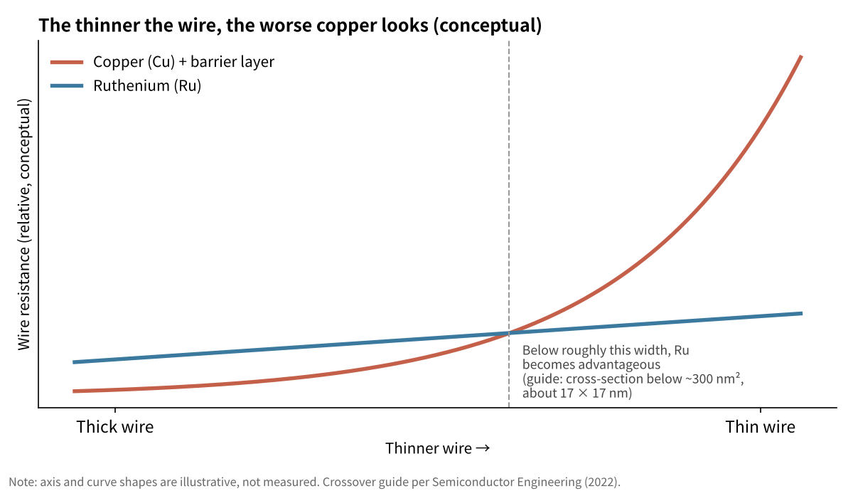
    As an interconnect material, copper becomes less attractive the thinner it gets. In a talk at IEDM 2020 (summarized in a series by EE Times Japan), imec compared the resistance of vias, the vertical connections between wiring layers. Taking a 14 nm copper via with a 2 nm barrier layer as the reference value of 1, a 10 nm copper via comes to 2.16, more than double, while ruthenium was calculated at 0.59 at 14 nm without a barrier layer. These are calculated comparisons that assume particular dimensions and structures, not direct measurements of actual products. Ruthenium is valued because its resistance is low, it does not need the barrier layer (a thin film that stops copper from diffusing into surrounding insulation) that copper requires, and it can be shaped by etching.

    Conceptual chart: copper resistance rises steeply as wires thin while ruthenium rises gently
    Conceptual schematic: not measured data. Crossover guide per Semiconductor Engineering (2022).

    imec’s 16 nm-pitch ruthenium lines

    On June 3, 2025, imec reported, in a presentation at the IITC 2025 conference, ruthenium lines at 16 nm pitch made with a semi-damascene process. The average resistance was 656 ohms per micrometer, and 40% of the 16 nm-pitch structures met the target resistance predicted from thin-film resistivity (corresponding to 8 nm-wide local wiring). At 18 to 22 nm pitch, full-wafer yield of more than 90% was reported. The work targets the first local wiring layer (M0) of logic chips from the A7 generation onward. This was a different conference from the VLSI Symposium presentation by Tokyo Electron and imec described above.

    Hurdles before real-world use

    Even in imec’s report, only 40% of structures at 16 nm pitch met the target resistance, and yields above 90% were obtained in the 18 to 22 nm pitch range. Remaining issues include optimizing the patterning of ruthenium and suppressing changes in its shape caused by heat. Replacing copper with ruthenium is still at the research stage.

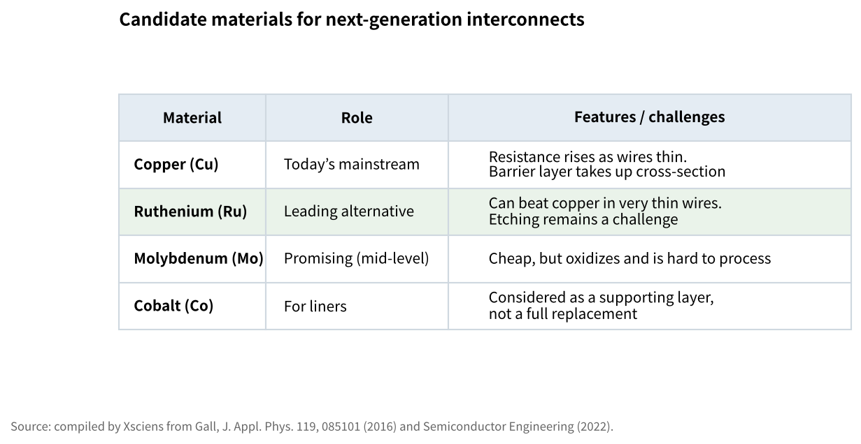
    Table of candidate interconnect materials: copper, ruthenium, molybdenum and cobalt
    Candidate materials and their roles (compiled by Xsciens from Gall 2016 and Semiconductor Engineering 2022).

    Xsciens Editorial Note

    “Copper to ruthenium” is not a done deal; it is a research question about where copper’s limit sits and which materials could take over beyond it.

    • Results versus mass production. What the conference presentations show are research-stage results. Independent work agrees that the direction is plausible: a materials study from Rensselaer Polytechnic Institute (Gall, 2016) found that some metals such as rhodium, iridium and nickel can outperform copper in very narrow wires, while molybdenum, cobalt and ruthenium roughly match it, so ruthenium is one candidate among several.
    • The crossover is a guide, not a line. A commonly cited guide is that ruthenium becomes less resistive than copper below a cross-section of roughly 300 nm² (about 17 × 17 nm), but the exact point depends on barrier thickness, grain structure and process. The figure in this article is a conceptual schematic, not measured data.
    • What to watch next. Etching without damaging the metal (oxidation is a known challenge), uniformity across a whole wafer, cost, and whether cheaper options such as molybdenum take the middle layers while ruthenium takes the thinnest ones.
    • Our imagination (speculation) — We wonder whether this kind of wiring change might eventually let phones and data centers do the same computing with less wasted heat, which could mean longer battery life or lower cooling needs. But a new material also brings new factory processes and costs, so how much of this reaches everyday products is still unknown. This is our speculation, not a forecast.

    References for this note: Gall, “Electron mean free path in elemental metals”, Journal of Applied Physics 119, 085101 (2016) (Rensselaer Polytechnic Institute), Semiconductor Engineering, “How Far Will Copper Interconnects Scale?” (Dec 15, 2022)

    Key terms

    • Pitch: the distance between the centers of neighboring wires
    • Via: a vertical connection between upper and lower wiring layers
    • Barrier layer: a thin film that keeps copper from diffusing into the surrounding insulating film
    • Superfill: deposition that fills even narrow trenches and gaps with metal evenly
    • A10, A7: names for next-generation chip nodes (the letter A stands for the angstrom, one tenth of a nanometer); they do not necessarily indicate an actual physical dimension

    Whether copper will actually be replaced by ruthenium in chip wiring remains a research question, not a settled fact. But tracking what gets presented at international conferences like this one reveals where the next bottlenecks in semiconductor scaling lie, and where equipment makers are looking for solutions. The unglamorous work of wiring a chip is turning out to be one of the front lines that will determine how far AI-era chip performance can go.

    Sources: Tokyo Electron Newsroom, “2025 IEEE Symposium on VLSI Technology and Circuits”, imec, “Semi-damascene metallization: an inflection point in back-end-of-line processing”, imec press release (June 3, 2025), EE Times Japan

  • [Science] How Low Protein Intake in Childhood Extends Lifespan: Drosophila (Fruit Fly) Study Reveals the Mechanism — RIKEN

    Many of us have heard some version of the idea that “what you eat as a child shapes your health as an adult.” The notion that nutrition during the fetal and early-life period influences later obesity, diabetes, and aging has long been recognized under the concept of DOHaD (Developmental Origins of Health and Disease). Yet exactly what happens inside the body to produce this effect has remained largely unknown. On September 24, 2026, a research team at Japan’s RIKEN institute announced that they had identified, in fruit flies, a molecule that offers a clue to solving this puzzle. The findings were published in the journal Nature.

    原論文情報 / Original Paper
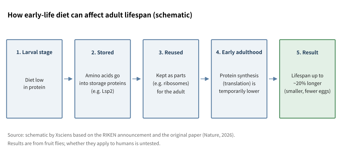
    Title: Lsp2 links early-life diet to adult translation and lifespan in Drosophila
    Authors: Kosakamoto, H. et al.
    Journal: Nature (2026)
    DOI: 10.1038/s41586-026-11031-3

    The experiment: change the diet only during the larval stage

    The research group (the Nutrient Response Research Team at RIKEN’s Center for Biosystems Dynamics Research, led by Team Director Fumiaki Obata, with Hina Kosakamoto and colleagues) fed fruit fly larvae a protein-restricted diet only during the larval stage, then returned the flies to a normal diet as adults and raised them for life. They combined chemically defined (synthetic) diets to control nutrition precisely, metabolic analysis, tracing of nutrients with stable isotopes (atoms that differ in mass but behave almost identically in chemistry), and genetic techniques.

    Result 1: Lifespan rose by up to about 20%

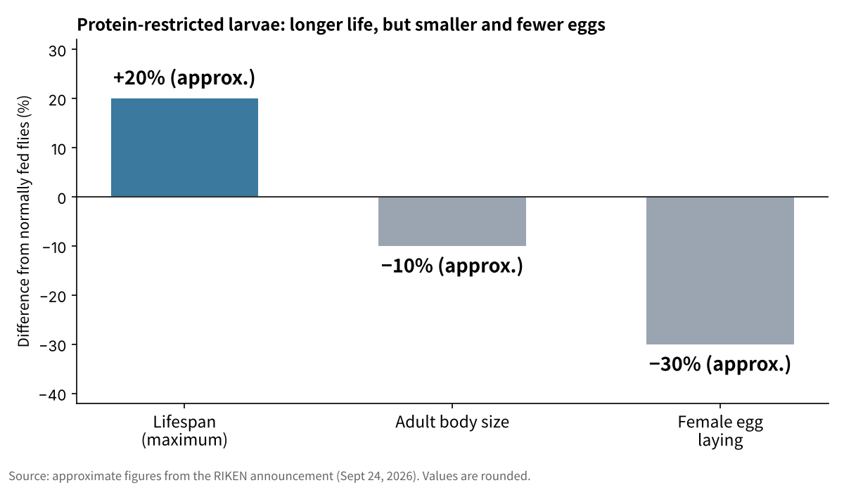
    Restricting protein only in the larval stage extended adult lifespan by up to roughly 20%, even though the adults ate a normal diet for the rest of their lives. The effect was seen in both males and females. Restricting only the amino acids in a synthetic larval diet gave a similar extension of up to about 20%. The benefit came with a cost: adults were about 10% smaller, and females laid roughly 30% fewer eggs. In other words, the longer life came with a trade-off against growth and reproduction.

    Bar chart: lifespan up about 20 percent, body size down about 10 percent, egg laying down about 30 percent
    Approximate differences from normally fed flies, based on the RIKEN announcement.

    Result 2: Larval amino acids were still in the adult body

    When the team tracked amino acids (the building blocks of proteins) labeled with stable isotopes, they found that amino acids taken up in the larval stage remained in many proteins after the flies became adults. In 6-day-old adults, about half of all proteins were still built from amino acids acquired during the larval stage. (The analysis used heads, where cell division has less influence on the result.) Larval amino acids were especially common in the parts of ribosomes, the molecular machines that make proteins inside cells.

    In flies that had been protein-restricted as larvae, early adults had fewer ribosomes and lower protein-synthesis activity (translation). This decline was limited to roughly the first week of adulthood; by day 14 the difference was gone. The researchers think this moderate, temporary suppression of translation is a major pathway behind the longer lifespan.

    Result 3: The key is a storage protein called Lsp2

    Amino acids taken up in the larval stage stay in the body as a storage protein called Lsp2, which is later reused as raw material for building new ribosomes in the early adult stage. When larvae were protein-restricted, Lsp2 levels fell, and the reduction persisted into early adulthood. Reducing Lsp2 alone by genetic knockdown (weakening the activity of a specific gene) lowered protein synthesis and extended lifespan just as dietary restriction did, and with almost no effect on body size or egg-laying. The team concludes that Lsp2 plays a central role in controlling lifespan.

    Lsp2 is rich in aromatic amino acids such as tyrosine and phenylalanine. Restricting just one of these amino acids in the larval diet was enough to reproduce the drop in Lsp2 and the longer lifespan. The team proposes a new mechanism in which a storage protein “remembers” early-life nutrition and carries that information into adulthood to regulate lifespan.

    Flow chart showing how larval diet leads to longer adult lifespan in fruit flies
    How early-life diet can affect adult lifespan (schematic by Xsciens based on the RIKEN announcement and the original paper).

    What it means for humans (and what it does not)

    The result offers a new lead for thinking about the molecular basis of the DOHaD hypothesis, which holds that nutrition in the fetal and infant period affects the risk of lifestyle-related disease in adulthood. RIKEN also raises the possibility that a decline in stored amino acids is read by the body as reduced nutrition, something like “eating until 80% full,” and mentions proteins that might play a similar role in humans, such as albumin and globulin in blood. Whether a similar mechanism exists in mammals remains to be tested.

    Because this work was done in fruit flies, it cannot be applied directly to human diets. The longer lifespan came with a smaller body and fewer eggs, so the finding does not mean that restricting a child’s diet would help them live longer.

    Xsciens Editorial Note

    The study offers a molecular clue that nutrients taken in early in life can persist in the body as building blocks into adulthood. It does not say that restricting children’s diets will make them live longer.

    • Separate what was observed from what was interpreted. What was observed: protein restriction in larvae extended adult lifespan by up to about 20%, and about half of all protein in the heads of 6-day-old adults came from larval amino acids. The idea that a temporary dip in early translation contributes to longer life is an interpretation drawn from experiments and genetics. “Up to” also means the gain can be smaller under other conditions.
    • Fly results, with costs. The longer-lived flies were about 10% smaller and females laid about 30% fewer eggs. The DOHaD hypothesis rests mainly on observational studies in humans, and whether this molecular mechanism exists in mammals is untested. Another group has reported that restricting larval diet also extends lifespan in flies, but that the effect depends strongly on the adult diet and works through a different route (lipid autotoxins), so longevity is unlikely to have a single mechanism.
    • What to watch next. Whether mammals have a similar “early nutrition stays in the body” mechanism, how timing and amount of restriction change the outcome, and whether the growth and fertility costs can be avoided.
    • Our imagination (speculation) — We wonder whether, if we learn where and how much of early-life nutrition stays in the body, it might become possible to spot health risks sooner in people who had a disadvantaged start, or to make up for it later. At the same time, the trade-off with body size and egg laying suggests the practical path is not “eat less” but finding ways to target only the parts that matter. This is only our speculation.

    References for this note: Stefana et al., Nature Communications (2017), “Developmental diet regulates Drosophila lifespan via lipid autotoxins” (Francis Crick Institute), Lacagnina, “The Developmental Origins of Health and Disease (DOHaD)”, American Journal of Lifestyle Medicine (2019)

    Key terms

    • DOHaD (Developmental Origins of Health and Disease): the idea that nutrition in the fetal and infant period affects health and disease risk in adulthood
    • Lsp2: a storage protein made in large amounts by fruit fly larvae that remains in the body into adulthood
    • Ribosome: the molecular machine in cells that makes proteins
    • Translation: the process of making proteins from genetic information (protein synthesis)
    • Knockdown: weakening the activity of a specific gene by genetic manipulation

    Sources: RIKEN press release, “The mechanism by which early-life nutrition determines lifespan” (September 24, 2026), Kosakamoto, H. et al. Nature (2026)