Tag: materials science

  • [Science] Hidden Crystal “Patchwork” Could Help Explain Why Superconductors Differ

    [Science] Hidden Crystal “Patchwork” Could Help Explain Why Superconductors Differ

    A copper-oxide superconductor that scientists have studied for about 40 years turns out not to be uniform inside. A University of Warwick team used 3D X-ray imaging to show that one well-known crystal is a patchwork of two slightly different atomic arrangements, divided by boundaries roughly 150 nanometres wide. That matters because most theories of these materials quietly assume a uniform crystal, and the hidden boundaries might help explain why seemingly identical samples can perform differently.

    原論文情報 / Original Paper
    Title: Giant Domain Walls and Intrinsic Heterogeneity in 214 Cuprate Superconductors
    Authors: Ladbrook, E., Wright, J. P., Senn, M. S.
    Journal: Physical Review Letters 137(12), 2026
    DOI: 10.1103/r62x-kt5j

    What the team found

    Copper-oxide superconductors, or cuprates, were discovered in 1986. They carry electricity with zero resistance at temperatures far higher than older superconductors, although still very cold by everyday standards. Four decades on, their behaviour remains only partly understood. Researchers have long known that cuprates can be uneven in their electronic behaviour, but many interpretations have still treated the underlying crystal structure as essentially the same all the way through. How different structural regions are arranged throughout the bulk of a crystal has remained unclear.

    The new study, led by Mark Senn at the University of Warwick with Evie Ladbrook and Jon Wright of the European Synchrotron Radiation Facility (ESRF) in France, tested that assumption directly. The sample was a tiny single crystal with the composition La₁.₆₇₅Eu₀.₂Sr₀.₁₂₅CuO₄. It belongs to the “214” family of copper-oxide compounds and is doped to one-eighth, meaning roughly one added charge carrier for every eight copper atoms in its copper-oxide layers, a level at which superconductivity is known to be fragile. Inside it, the researchers found regions with two closely related atomic arrangements, separated by walls far broader than expected.

    How you photograph the inside of a crystal

    The tool was scanning 3D X-ray diffraction, which works a little like a CT scan. At ESRF’s ID11 beamline, the team focused an X-ray beam to about 120 nanometres and scanned it across the crystal in 50-nanometre steps. The crystal was also rotated so that diffraction data came from many angles, and each scan took about two hours. From the positions of the diffraction spots, the team reconstructed how the crystal lattice is stretched or twisted from place to place, with a strain sensitivity of roughly two parts in ten thousand. Beyond superconductors, the same approach could be used to look for hidden structural variations in other complex materials.

    The Warwick press release credits a recent €150 million upgrade of the ESRF for making this kind of measurement practical. In the paper’s own words, the technique offers a general way to resolve the bulk microstructure of materials, not just superconductors.
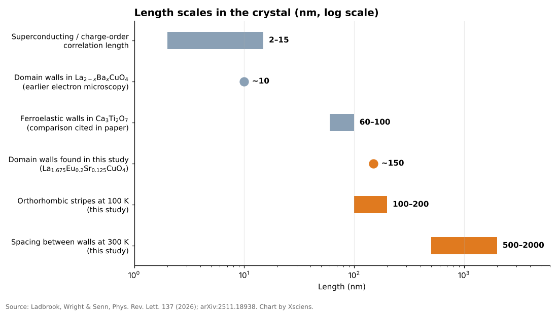
    Bar chart on a log scale comparing the 150 nm domain walls found in this study with other length scales in cuprates
    Source: Ladbrook, Wright and Senn (2026), Physical Review Letters; arXiv:2511.18938. Chart by Xsciens.

    Walls broader than anyone expected

    At room temperature (300 K) the crystal is mostly in a so-called orthorhombic state, in which the lattice is slightly stretched along one in-plane direction, with two orientations of twin domains (regions of the same structure rotated relative to each other) each a micron or more across. Between them the team saw wall regions about 150 nanometres thick, spaced roughly 0.5 to 2 micrometres apart, where the measured orthorhombic strain approaches zero. In other words, the walls look more like a different, tetragonal-like structure, one with equal lengths along both in-plane directions, than like thin seams between two orthorhombic domains.

    For comparison, earlier electron-microscopy work on a related compound, La₂₋ₓBaₓCuO₄, estimated the width of similar regions at only around 10 nanometres, and the correlation lengths of superconducting and charge-density-wave order in cuprates are typically about 2 to 15 nanometres. (Charge order is a pattern in which electrons gather in regularly repeating regions instead of spreading evenly.) The comparison is rough, since the compounds and techniques differ, but it suggests the new walls are not tiny imperfections: they are broad enough to behave almost like a structure in their own right. Professor Senn said that for forty years the working assumption had been that these materials are the same all the way through.

    Cooling reshapes the pattern

    The picture changes as the crystal is cooled. This material is known to switch around 160 K from the orthorhombic state to a low-temperature tetragonal one, and the team measured it at 300, 140, 120 and 100 K. At 100 K they saw the reverse arrangement: fine stripes of orthorhombic-like material, each roughly 100 to 200 nanometres wide, embedded in a tetragonal matrix. So the pattern does not simply become more uniform on cooling; the dominant structure changes while smaller regions of the other one remain embedded in it. Earlier studies have reported that this kind of coexistence persists down to at least 10 K in this material and a related barium compound, but the new X-ray measurements went no lower than 100 K.
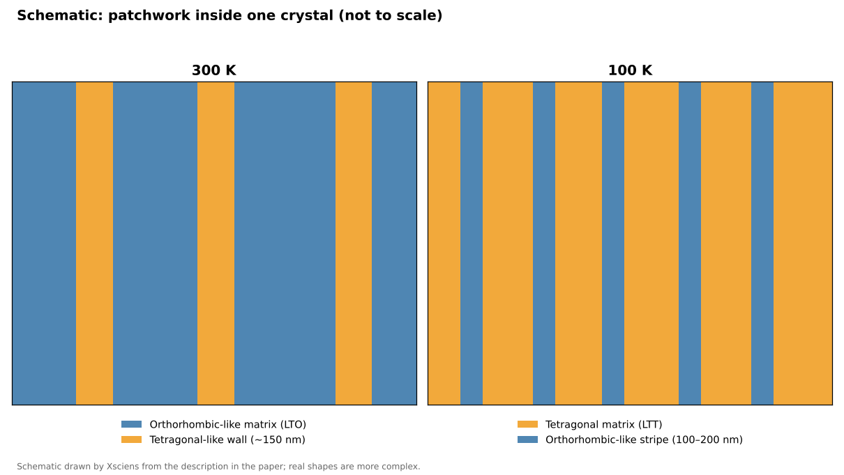
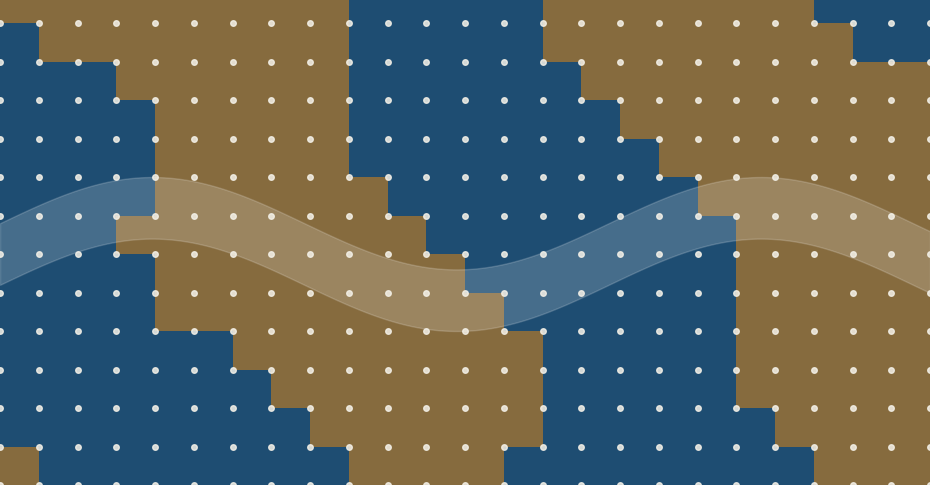
    Schematic showing tetragonal-like walls in an orthorhombic matrix at 300 K and orthorhombic-like stripes in a tetragonal matrix at 100 K
    Schematic by Xsciens based on the description in the paper; not to scale.

    Why it matters, and what is not yet shown

    The idea that structure and superconductivity interact in this family is not new. In 1995, a neutron-scattering study on a related compound near one-eighth doping linked a static pattern of alternating spin and charge stripes to the suppression of superconductivity there. What the Warwick work adds is a three-dimensional, micrometre-scale view of how the crystal structure itself is divided up, and the finding that the dividing walls are much wider than the sharp seams people tended to picture.

    The authors suggest the tetragonal-like boundaries could influence the competition between superconductivity and charge order, and Professor Senn says they probably work against superconductivity rather than alongside it. If so, that could help explain why some cuprates outperform others and why bulk measurements sometimes disagree. Understanding why some cuprates superconduct better than others has been a longstanding challenge, so the way structural regions are arranged may be one more factor to consider alongside chemical composition. The authors also expect similar patchwork in the wider 214 family, and possibly in related materials studied under extreme pressure. If so, some past bulk measurements may need reinterpreting.

    Those are hypotheses, not results. The experiment measured crystal structure, not electrical behaviour: superconductivity at the walls was not measured directly, and the paper describes the link as suggestive. Only one micro-crystal was measured, the apparent wall width depends on the instrument’s resolution, and the faint charge-order signals cannot yet be mapped with this method.

    Xsciens Editorial Note

    One carefully imaged crystal shows that the “same all the way through” assumption fails in at least one well-studied cuprate.

    • What was observed versus what was inferred. The observation is a three-dimensional map of structural distortion: tetragonal-like walls about 150 nm thick at 300 K and orthorhombic-like stripes in a tetragonal matrix at 100 K. That the walls suppress superconductivity is an interpretation, not a direct measurement, and the paper calls the evidence suggestive.
    • The sample is tiny and single. The result comes from one crystal about 15 × 20 × 20 micrometres of one composition. The authors state that extending it to other cuprates is a prediction, and measured wall widths depend on the instrument’s resolution (roughly 30–70 nm).
    • What to watch next. The key test is whether superconductivity is weaker inside the walls themselves or whether the walls affect the surrounding crystal. That needs structural imaging combined with local electrical measurements, including charge order, repeated on other cuprates.
    • From the editors — superconductors that are easier to make and work better could one day mean leaner power grids and smaller, cheaper MRI scanners in more hospitals. The route there may run through treating the arrangement of a crystal’s internal regions as a design dial, alongside its chemical recipe, although removing every wall might not even help. But a tidy lab crystal is a long way from an affordable wire. So when a superconductor headline promises a revolution, ask how large the sample was and what was actually measured.

    References for this note: Keimer et al., “From quantum matter to high-temperature superconductivity in copper oxides,” Nature (2015), Tranquada et al., “Evidence for stripe correlations of spins and holes in copper oxide superconductors,” Nature (1995)

    Sources: University of Warwick press release, Physical Review Letters (DOI 10.1103/r62x-kt5j), arXiv:2511.18938

  • [Science] What Is a Supramolecular Polymer? A Simple Guide to How It Works

    [Science] What Is a Supramolecular Polymer? A Simple Guide to How It Works

    A supramolecular polymer is a chain-like material whose building blocks link up through weak, reversible attractions instead of strong, fixed chemical bonds. That “weak but many” design can let these materials repair damage, change shape, and influence how living cells grow — which is why materials scientists have been racing to build bigger, more precisely controlled versions of them.

    What Is a Supramolecular Polymer?

    A conventional polymer — the plastic in a water bottle, for example — is a long chain of small repeating units called monomers, welded together end-to-end by covalent bonds. Covalent bonds are the strong, electron-sharing connections that hold most everyday molecules together, and once formed they generally don’t come apart on their own.

    A supramolecular polymer (a term built from “supra-,” meaning “beyond,” plus “molecular”) swaps those permanent welds for temporary handshakes. Its monomers link up through noncovalent interactions — hydrogen bonds, stacked ring structures, metal-ion bridges, or simple electrical attraction — that are individually weak but, strung together by the thousands along a chain, add up to a stable, functional material. A useful everyday comparison is Velcro: a single hook-and-loop pair peels apart with almost no effort, but a whole strip of them holds a heavy jacket closed. Supramolecular polymers work the same way at the molecular scale — weak links in large numbers behave like a strong, yet reversible, material.

    IUPAC’s 2013 polymer-science recommendations favor the term “supramolecular association” (also called “Lehn association,” after chemist Jean-Marie Lehn) for this self-assembly process, and discourage the related term “supramolecular polymerization.” That is a naming preference for the process, not a rejection of the material-class name: “supramolecular polymer” remains the term used throughout the chemistry and materials literature — including in the title of the 2026 Northwestern University paper described below — so this article uses it in that common sense.

    How the Self-Assembly Works

    Because the bonds holding a supramolecular polymer together are reversible, individual connections continually break and re-form, letting the material adjust to its surroundings without necessarily falling apart. When the damaged surfaces of such a material can come back into contact and the molecules are mobile enough, those reversible interactions can reconnect across the damage — the basis for self-healing in some (not all) supramolecular materials; how well it works depends heavily on the specific design. According to a 2024 overview from the Society of Plastics Engineers, this same dynamic bonding can also let certain supramolecular polymers flow or be reshaped more easily than conventional plastics, though the exact processing temperature and pressure still depend on the molecular design in question.

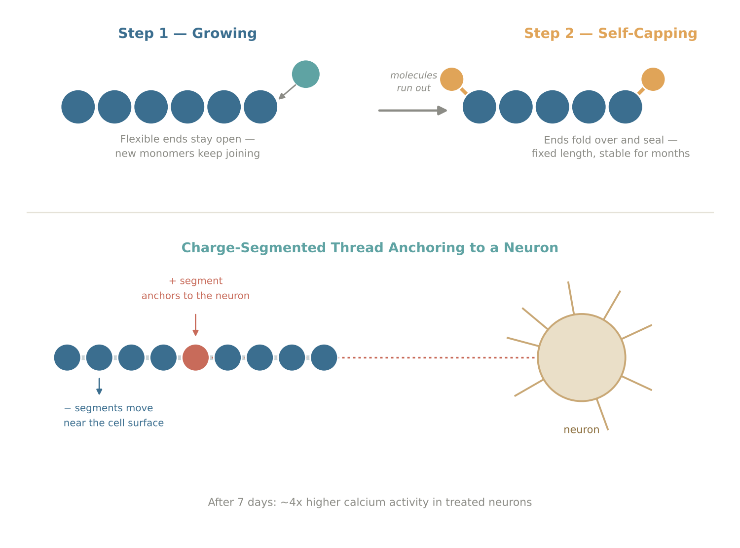
    Chemists have also learned to design chains that grow to a controlled length and then stop. One such strategy, demonstrated in an October 2026 study from Northwestern University, is called self-capping supramolecular polymerization. The molecular design lets a growing thread’s flexible ends keep adding building blocks while conditions allow it, then fold over and form a cap that limits further growth. Introducing a fresh batch of building blocks can restart the process, which lets researchers extend the assembly and arrange distinct segments along its length.

    Getting this right is a balancing act. If the building blocks do not bind to each other strongly enough under the given conditions, only short, unstable clusters form. If the interactions are too strong, the material can lose the ability to rearrange that makes supramolecular polymers useful in the first place. Scientists must also keep growing chains from fusing together unpredictably or slowly falling back apart — failure modes that, together with this binding-strength trade-off, are much of what makes precise supramolecular engineering difficult.

    Why It’s Getting Attention Now

    Supramolecular polymers have been studied since the late 1980s. In 1988, chemist Takuzo Aida and colleagues reported one of the field’s early milestones: disc-shaped porphyrin molecules that stacked face-to-face into one-dimensional assemblies through noncovalent interactions. Chemist Jean Fréchet’s group then used hydrogen bonds to build liquid-crystalline supramolecular structures in 1989, and Nobel laureate Jean-Marie Lehn’s group demonstrated hydrogen-bonded, liquid-crystalline supramolecular polymers in 1990. Chemist Bert Meijer’s widely cited 1997 work on four-point hydrogen-bonded monomers then showed that noncovalent assemblies could behave mechanically like true high-molecular-weight polymers. What has changed since then is precision: for decades, supramolecular polymers tended to form with uneven, hard-to-control lengths, which limited how reliably their properties could be engineered for a specific application.

    That is the gap the Northwestern team, led by materials scientist Samuel I. Stupp with postdoctoral fellow Michael Dore and graduate students Simon Egner and Madison Strong, targeted in a study published October 1, 2026, in the journal Science. Using self-capping, they built threads with molar masses reaching into the billions of daltons — roughly 100 times heavier, by the university’s own comparison, than large conventional polymers or the largest known natural proteins, with the longest threads wider than a single cell. According to the researchers, the threads kept their controlled length for months in a test tube without clumping, merging, or dissolving back apart under the tested conditions, something earlier, less-controlled supramolecular polymers struggled to do.

    “That introduces a very different way of thinking about how materials can communicate with cells,” said Northwestern’s Samuel I. Stupp of the findings.

    Diagram showing self-capping supramolecular polymerization and a charge-segmented thread anchoring to a neuron
    Source: created based on Dore et al., Science (2026) and Northwestern University’s press release.

    Uses: Self-Healing Plastics to Neurons

    The reversible bonding at the heart of supramolecular polymers already points toward several practical uses. Self-healing coatings and parts for construction, automotive, and aerospace use could extend equipment lifespans by letting small cracks mend themselves rather than requiring replacement. Stimuli-responsive versions are being explored as drug-delivery carriers that release their cargo only when they encounter a specific biological trigger, such as a change in pH inside the body, and supramolecular hydrogels — soft, water-swollen networks — are used as scaffolds in tissue engineering to support growing cells. Researchers are also testing supramolecular designs in adaptive coatings that resist corrosion and wear, and in soft robotics, where flexible, responsive materials can mimic the give-and-take of biological tissue.

    The Northwestern study adds a striking new example. The team tested several charge patterns on neurons grown in lab dishes: threads made entirely of positively charged segments harmed the cells, threads made entirely of negative segments had little effect, and randomly mixed charges produced no notable response. Only one design worked well — a short positively charged segment sandwiched between two longer negatively charged segments, which anchored the thread to the negatively charged neuron surface. In that condition, neurons showed roughly four times more measured calcium activity (an indicator of cellular signaling, though not a direct measure of overall neuronal function) after one week, and had formed more synaptic connections by two weeks, without the researchers adding any conventional biological growth factors. The researchers caution that this is cell-culture work only, with no animal or human testing yet, so any medical application for nerve repair remains a long-term prospect rather than a near-term product.

    What to Watch Next

    Market research firm Transparency Market Research estimated the global supramolecular polymer market at roughly $291.5 million in 2024, projecting about 6.5% annual growth through 2031. The more scientifically telling milestone to watch, though, is whether precisely built, billion-dalton threads like Northwestern’s can be scaled up and tested in living animals, not just lab dishes.

    For more on the specific billion-dalton threads discussed above and how they boosted nerve-cell activity in the lab, see our related article: Scientists Build a Billion-Dalton Molecular Thread Longer Than a Cell.

    Sources: Northwestern University (Weinberg College), EurekAlert! press release, IUPAC Gold Book

  • [Science] Scientists Build a Billion-Dalton Molecular Thread Longer Than a Cell — It Quadrupled Nerve-Cell Activity in the Lab

    [Science] Scientists Build a Billion-Dalton Molecular Thread Longer Than a Cell — It Quadrupled Nerve-Cell Activity in the Lab

    • A newly built, self-assembling material made nerve cells growing in a lab dish roughly four times more biologically active than usual, hinting that materials like it could one day help repair damaged nerves.
    • Chemists at Northwestern University found a new way to precisely control how long a certain kind of molecular thread grows, and how its positively and negatively charged segments are arranged along the way.
    • By molecular standards the resulting threads are enormous — roughly 100 times heavier than typical plastic-like polymers and bigger than even the largest proteins found in nature — even though they are built from many smaller molecules that click together on their own, rather than one molecule held together by ordinary chemical bonds.
    • So far the effect has only been shown in cells grown in a lab dish, not in animals or people, so any real treatment is still a long way off.

    Billion-Dalton Supramolecular Polymers: A Structure Big Enough to Rival a Cell

    A team led by the chemist Samuel I. Stupp at Northwestern University has built a new kind of giant structure, described in the journal Science on October 1, 2026. It belongs to a class of materials called supramolecular polymers. Rather than being a single molecule held together by strong chemical bonds the way an ordinary plastic is, it is made of many smaller molecules that click onto one another and hold themselves together more loosely, the way a line of magnets snaps together end to end. That looseness usually makes supramolecular polymers easy to assemble but hard to control, since there has been no reliable way to stop them from growing at a chosen point.

    Scientists weigh molecules in daltons, a unit named after the 19th-century chemist John Dalton, where one dalton is roughly the mass of a single hydrogen atom. Northwestern researchers point to common high-mass synthetic polymers used in materials science, which weigh around 10 million daltons, for comparison. Some of the largest proteins found in nature — the kind that give muscle tissue its structure — are in the roughly 3 to 5 million-dalton range. The new Northwestern assembly reaches a combined mass in the billions of daltons, around 100 times heavier than those conventional polymers, and its longest threads stretch farther than the width of a single living cell.

    Bar chart comparing molecular weight of a natural protein, a conventional polymer, and the new Northwestern assembly on a log scale
    Figure 1. Molecular weight on a log scale: a natural protein, a conventional polymer and the new billion-dalton supramolecular polymer. Source: data from Dore et al., Science (2026); Northwestern University

    Why Controlling the Length Was So Hard

    Because supramolecular polymers assemble themselves from many separate molecules rather than being built link by link under a chemist’s control, they have historically kept growing in a somewhat unpredictable way. That made it hard to control how long any given thread would grow, or where along its length particular features would end up. The Northwestern team solved this with a technique they call self-capping supramolecular polymerization: as the supply of available building-block molecules runs low, flexible regions at each end of the growing thread fold over on themselves, effectively capping the ends and stopping further growth.

    That trick let the researchers control two things at once: the overall length of each thread, and how positively and negatively charged segments are arranged along it. In a statement describing the work, Stupp called the result a breakthrough in materials design.

    “We discovered something we had never seen before in chemistry or in biology.”

    Precise Length and Charge Segmentation: The Charge Pattern Made the Difference

    Before arriving at their final design, the researchers tried several simpler charge patterns on neurons growing in a lab dish. Threads carrying only positive charge essentially killed the neurons; threads carrying only negative charge did almost nothing; and threads with positive and negative charge mixed randomly along their length produced no notable response either. Only one design worked well: a short positively charged segment flanked by longer negatively charged segments, arranged with precision rather than left to chance.

    To see how this winning design affected living neurons in culture, the researchers added it to cells growing in a lab dish and tracked them over 7 and 14 days. They used a technique called calcium imaging, which tracks what is known as calcium activity — a widely used indicator of how active a nerve cell is, since neurons briefly let calcium ions flow across their outer membrane as part of firing a signal. It is a standard, well-established way for researchers to gauge neural activity, though it is an indirect measure rather than a literal count of signals fired.

    Neurons treated with the winning design showed overall calcium activity roughly four times greater than untreated neurons after seven days, and had formed more synapses by 14 days. The researchers propose that the precise charge pattern works by shaping how the material interacts with the neurons’ outer membrane and with proteins around it, though they describe this as a proposed mechanism rather than a fully confirmed one. Notably, the effect appeared without adding any separate drug, growth factor, or other biological signaling molecule — the geometry of the charge pattern alone was enough to measurably change how the cells behaved.

    That matters because nerve cells are known to rely on their electrical activity, along with other cues, to grow new branches and form synapses, the junctions where one neuron passes a signal to the next. Materials associated with more active, better-connected neurons are therefore of particular interest for regenerative medicine, the branch of science focused on helping the body rebuild tissue it has lost or damaged, including nerve tissue after an injury. The researchers describe the link between an entirely synthetic, self-assembling material and this kind of change in living cells as the most surprising part of the result.

    Bar chart showing neurons treated with the new material had four times the calcium activity of untreated neurons
    Figure 2. Neurons treated with the new material showed about four times the calcium activity of untreated neurons. Source: data from Dore et al., Science (2026); Northwestern University

    From a Lab Dish to a Possible Therapy

    So far this particular design has only been tested on neurons growing in a dish, not in animals or people, so any medical use is still likely years away. Lab-dish results are a long way from a treatment: cells in a dish do not have to survive inside a living body, fight off an immune response, or integrate with surrounding tissue the way they would after an actual injury. The Stupp lab has, however, spent years designing self-assembling materials aimed at nerve repair and tissue regeneration, and the researchers see this new level of precision as a step toward building more reliable, tunable materials for that purpose. A logical next stage would be testing whether the material remains safe and effective in animal models of nerve damage, before any human study could even be considered.

    The achievement also matters well beyond medicine. Being able to build a giant synthetic structure with a chosen length and a precisely controlled charge pattern opens the door to new materials with tunable mechanical or electrical behavior, useful in fields far from biology too. More broadly, it shows how self-assembly can be used to control a material’s properties over distances far larger than a single molecule — a step toward manufacturing matter with a level of precision that has mostly been limited, until now, to much smaller scales.

    Sources: Northwestern Now, EurekAlert!

    Paper: Dore, M. et al., “Precise length and charge segmentation of billion-dalton supramolecular polymers”, Science (2026).

    Related: new to the topic? Start with What Is a Supramolecular Polymer? A Simple Guide to How It Works.

  • [Science] Beyond Copper: The Battle Over Next-Generation Chip Interconnects

    Inside every semiconductor chip, transistors are wired together by interconnects thinner than one ten-thousandth the width of a human hair. Copper (Cu) has been the workhorse material for these wires for decades, but it is now running into a physical wall as chips keep shrinking. At the VLSI Symposium, an international conference held in Kyoto in June 2025, Tokyo Electron and imec, the Belgium-based research institute, jointly presented new research into what could replace copper in future chips. Their presentation offers a window into where interconnect technology is headed next.

    Why copper wiring is nearing its limit

    Copper has long been the default choice for on-chip wiring because it conducts electricity well and is relatively easy to process. But once wire widths shrink to around 40 nanometers (nm; one nanometer is one-billionth of a meter) or below, copper’s resistance actually starts to rise rather than fall. As wires get thinner, electrons collide more often with the wire’s surface and with the boundaries between metal grains, making it harder for current to flow smoothly. Higher resistance means slower signals and higher power consumption. Since further miniaturization is inevitable, finding a replacement for copper has become a shared challenge across the industry.

    The presentation: ruthenium and semi-damascene wiring

    The joint presentation by Tokyo Electron and imec at VLSI 2025 was titled “Selective Deposition and Ruthenium Superfill for A10-and-Beyond Interconnects.” Ruthenium (Ru) is drawing attention as a metal whose resistance rises more gradually than copper’s as wires get thinner.

    The key idea is a fabrication approach called “semi-damascene.” Conventional copper wiring has relied mainly on the “damascene” process: a trench is etched into the insulating layer first, then filled with metal, and the surface is polished flat. Semi-damascene works differently. A metal film is first deposited across the entire wiring layer, and the unwanted portions are then removed by etching to directly carve out the wiring pattern, skipping the trench-and-fill step altogether. This makes it easier to build the finer, more three-dimensional wiring structures that future chips will need. The new presentation outlined a technical path for depositing ruthenium evenly, even into the narrowest gaps, when this process is used, a property known as “superfill.”

    Why this matters

    In AI chips packed densely with computing circuits, power loss and signal delay in the interconnects can limit the performance of the entire chip. The fact that Tokyo Electron, an equipment maker, is co-developing the interconnect process itself with imec, a materials research hub, signals something important: the practical realization of next-generation interconnects is no longer just about sourcing the right material, it has become a contest over deposition and processing equipment technology.

    AI computation depends on huge numbers of transistors exchanging large amounts of data. Even if transistors get faster, high wire resistance delays signals and increases heat and power use. Interconnects are like the roads of a chip, and their quality helps determine overall performance. That is why the search for a copper replacement is as important to semiconductor progress as transistor scaling itself.

    Why ruthenium looks promising

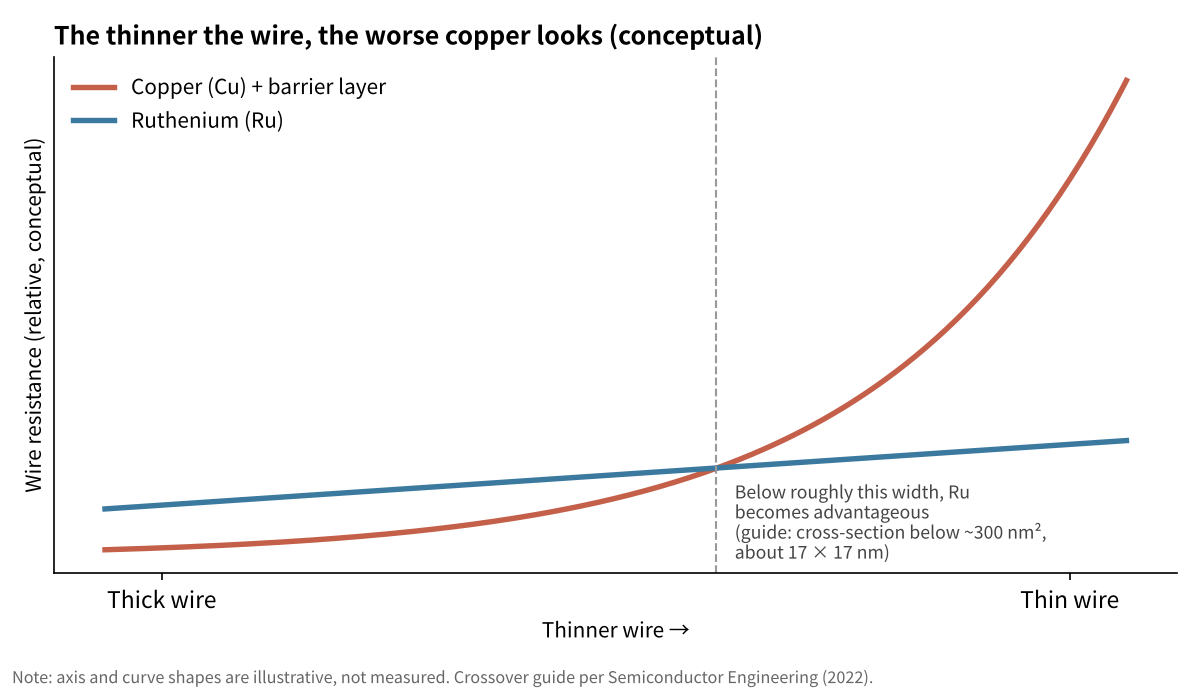
    As an interconnect material, copper becomes less attractive the thinner it gets. In a talk at IEDM 2020 (summarized in a series by EE Times Japan), imec compared the resistance of vias, the vertical connections between wiring layers. Taking a 14 nm copper via with a 2 nm barrier layer as the reference value of 1, a 10 nm copper via comes to 2.16, more than double, while ruthenium was calculated at 0.59 at 14 nm without a barrier layer. These are calculated comparisons that assume particular dimensions and structures, not direct measurements of actual products. Ruthenium is valued because its resistance is low, it does not need the barrier layer (a thin film that stops copper from diffusing into surrounding insulation) that copper requires, and it can be shaped by etching.

    Conceptual chart: copper resistance rises steeply as wires thin while ruthenium rises gently
    Conceptual schematic: not measured data. Crossover guide per Semiconductor Engineering (2022).

    imec’s 16 nm-pitch ruthenium lines

    On June 3, 2025, imec reported, in a presentation at the IITC 2025 conference, ruthenium lines at 16 nm pitch made with a semi-damascene process. The average resistance was 656 ohms per micrometer, and 40% of the 16 nm-pitch structures met the target resistance predicted from thin-film resistivity (corresponding to 8 nm-wide local wiring). At 18 to 22 nm pitch, full-wafer yield of more than 90% was reported. The work targets the first local wiring layer (M0) of logic chips from the A7 generation onward. This was a different conference from the VLSI Symposium presentation by Tokyo Electron and imec described above.

    Hurdles before real-world use

    Even in imec’s report, only 40% of structures at 16 nm pitch met the target resistance, and yields above 90% were obtained in the 18 to 22 nm pitch range. Remaining issues include optimizing the patterning of ruthenium and suppressing changes in its shape caused by heat. Replacing copper with ruthenium is still at the research stage.

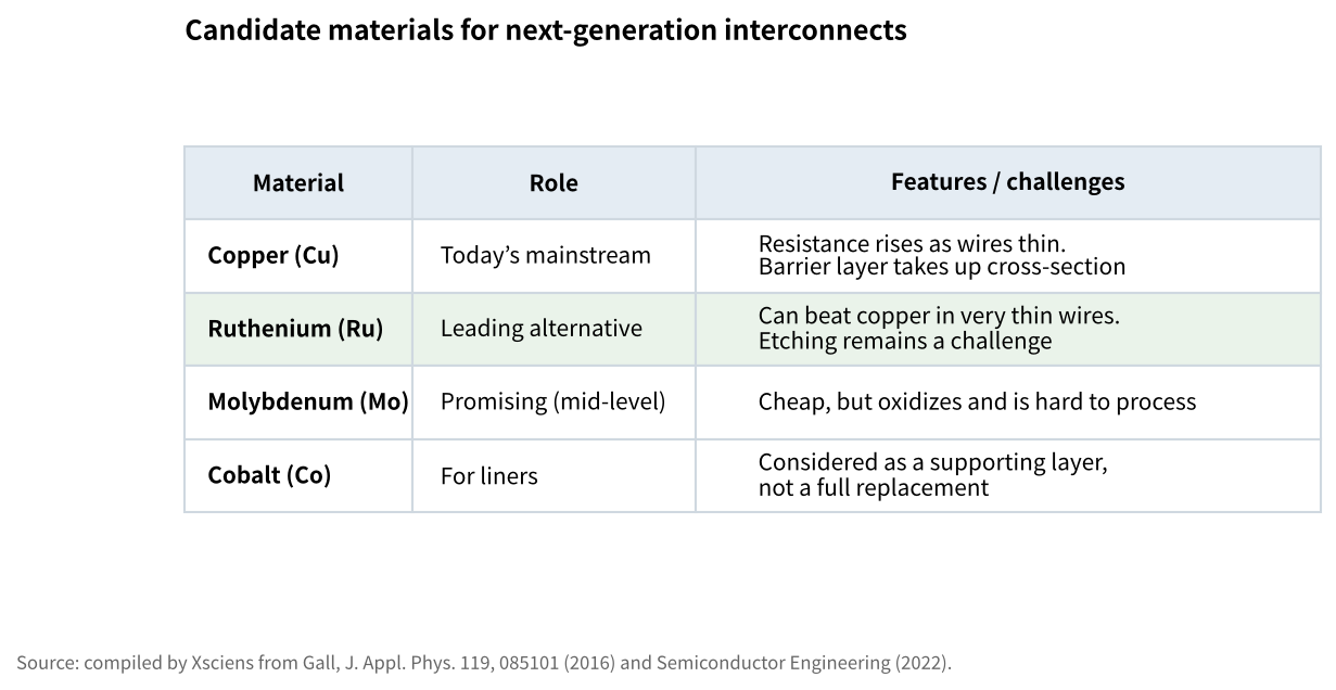
    Table of candidate interconnect materials: copper, ruthenium, molybdenum and cobalt
    Candidate materials and their roles (compiled by Xsciens from Gall 2016 and Semiconductor Engineering 2022).

    Xsciens Editorial Note

    “Copper to ruthenium” is not a done deal; it is a research question about where copper’s limit sits and which materials could take over beyond it.

    • Results versus mass production. What the conference presentations show are research-stage results. Independent work agrees that the direction is plausible: a materials study from Rensselaer Polytechnic Institute (Gall, 2016) found that some metals such as rhodium, iridium and nickel can outperform copper in very narrow wires, while molybdenum, cobalt and ruthenium roughly match it, so ruthenium is one candidate among several.
    • The crossover is a guide, not a line. A commonly cited guide is that ruthenium becomes less resistive than copper below a cross-section of roughly 300 nm² (about 17 × 17 nm), but the exact point depends on barrier thickness, grain structure and process. The figure in this article is a conceptual schematic, not measured data.
    • What to watch next. Etching without damaging the metal (oxidation is a known challenge), uniformity across a whole wafer, cost, and whether cheaper options such as molybdenum take the middle layers while ruthenium takes the thinnest ones.
    • Our imagination (speculation) — We wonder whether this kind of wiring change might eventually let phones and data centers do the same computing with less wasted heat, which could mean longer battery life or lower cooling needs. But a new material also brings new factory processes and costs, so how much of this reaches everyday products is still unknown. This is our speculation, not a forecast.

    References for this note: Gall, “Electron mean free path in elemental metals”, Journal of Applied Physics 119, 085101 (2016) (Rensselaer Polytechnic Institute), Semiconductor Engineering, “How Far Will Copper Interconnects Scale?” (Dec 15, 2022)

    Key terms

    • Pitch: the distance between the centers of neighboring wires
    • Via: a vertical connection between upper and lower wiring layers
    • Barrier layer: a thin film that keeps copper from diffusing into the surrounding insulating film
    • Superfill: deposition that fills even narrow trenches and gaps with metal evenly
    • A10, A7: names for next-generation chip nodes (the letter A stands for the angstrom, one tenth of a nanometer); they do not necessarily indicate an actual physical dimension

    Whether copper will actually be replaced by ruthenium in chip wiring remains a research question, not a settled fact. But tracking what gets presented at international conferences like this one reveals where the next bottlenecks in semiconductor scaling lie, and where equipment makers are looking for solutions. The unglamorous work of wiring a chip is turning out to be one of the front lines that will determine how far AI-era chip performance can go.

    Sources: Tokyo Electron Newsroom, “2025 IEEE Symposium on VLSI Technology and Circuits”, imec, “Semi-damascene metallization: an inflection point in back-end-of-line processing”, imec press release (June 3, 2025), EE Times Japan